Igor GUSEV, Andrey MARKITANOV
Gavrila was an audiophile,
Gavrila created DACs...
Indeed, why don’t we make a DAC ourselves? Is this necessary at all? Certainly! An external converter will be useful, first of all, to owners of CD players released 5 - 10 years ago. Digital audio processing technology is developing at a rapid pace, and the idea of reviving the sound of an old but beloved device using an external DAC seems very tempting. Secondly, such a device can be of great benefit to those who have an inexpensive model equipped with a digital output - this is a chance to take their sound to a new level.
It’s no secret that when creating an inexpensive CD player, the developer is within strict financial limits: he needs to choose a decent vehicle, equip the new product with every service to the maximum, display more buttons with a multifunction indicator on the front panel, etc., otherwise Due to the strict laws of the market, the device will not be sold. In a year, as a rule, a new one will appear, which is sometimes no better in sound than the old one (and often worse), and so on ad infinitum. And most large companies usually change the entire model range every spring...
The allocated funds are usually not enough for a high-quality DAC and the analog part of the circuit, and many manufacturers openly save money on this. There are, however, exceptions to this rule when such decisions are made deliberately, as an element of the company’s technical policy.
For example, the Japanese S.E.S., well known to our audiophiles. puts in its models CD2100 and CD3100 expensive transport with a large number of manual adjustments, while using a simple DAC, which clearly does not correspond to the class of mechanics. These devices are positioned by the company as transport with a control audio path and are initially designed to work with an external converter. The situation is somewhat different with the TEAC VRDS 10 - 25 players. By installing a high-quality drive and expensive TDA1547 (DAC 7) DAC chips, the engineers for some reason decided to save on the output stages. One Russian company, knowing about this feature of the models, makes an upgrade, replacing the analog part of the circuit.
About the authors
Andrey Markitanov, engineer at the Three V Sound Engineering Design Bureau from Taganrog. Develops and puts into production DACs under the Markan brand, and is a regular participant in Russian Hi-End exhibitions. He loves non-standard solutions, follows audio fashion, and is always up to date with the latest advances in the field of digital circuitry. He knows by heart the pinouts of many Crystal, Burr-Brown and Philips chips.
A little theory
So, it’s decided - we’ll make a DAC. Before we start looking at the diagram, it would be useful to decipher some generally accepted abbreviations:
S/PDIF (Sony/Philips Digital Interface Format)- standard for digital transmission of audio data between devices (asynchronous interface with self-synchronization). There is also an optical variant called TosLink (from Toshiba and Link). Almost all models of inexpensive CD players are equipped with this interface, but it is now considered obsolete. There are more advanced interfaces used in expensive devices, but we won’t talk about them yet.
DAC (DAC)- digital-to-analog converter.
IIS (Inter IC Signal bus)- standard for a synchronous interface between circuit elements within the same device.
PLL (Phase Locked Loop)- phase-locked loop system.
Emphasis- pre-emphasis.
Currently, there are two completely different digital-to-analog conversion methods for the CD Audio format: single-bit and multi-bit. Without going into detail about each of them, we note that the vast majority of expensive DAC models use multi-bit conversion. Why expensive? For a decent implementation of this option, a high-quality multi-channel power supply is required, a complex procedure for setting up output filters, in some models this is done manually, and in developed countries the work of a qualified specialist cannot be cheap.
However, single-bit converters also have many fans, because they have a unique sound delivery character, some features of which are difficult to achieve using existing multi-bit technology. These include the higher linearity of single-bit DACs at low signal levels, and therefore better microdynamics and clear, detailed sound. In turn, the argument of supporters of multibit DACs is a stronger emotional impact on the listener, the scale and openness of the sound, which are perfectly reproduced by the so-called. “drive” and “ches”, which are especially appreciated by rock lovers.
In theory, single-bit DACs require a very high clock speed to operate flawlessly. In our case, i.e. 16 bits and 44.1 kHz, it should be around 2.9 GHz, which is a completely unacceptable value from a technical point of view. With the help of mathematical tricks and various recalculations, it can be reduced to acceptable values within a few tens of megahertz. Apparently, this explains some of the sound features of single-bit DACs. So which one is better? We will describe both options, and decide for yourself which one to choose.
The main thing that guided us when developing the circuit was its extreme simplicity, which allows even an audiophile who is not experienced in digital technology to understand the idea and implement it in a specific design. However, the described DAC is capable of significantly improving the sound of a budget device equipped with a coaxial digital output. If your player does not have one, then it will not be difficult to organize it yourself. To do this, in most cases, it is enough to install an RCA connector on the back wall and solder its signal lobe to the corresponding place on the board. As a rule, the basic version of the motherboard is made for several models at once, only it is “packed” in different ways, and there must be space on it for soldering a digital output socket. If this is not the case, you will have to look for a diagram of the device - in authorized service centers, on radio markets or on the Internet. In the future, this layout can serve as the object of efforts to further improve it and will finally allow us to achieve “a gentle haze over a clean image.”
Almost all devices of this type are built on a similar element base; the choice of elements for the developer is not so wide. Among those available in Russia, let's name microcircuits from Burr-Brown, Crystal Semiconductors, Analog Devices, Philips. Among the S/PDIF signal receivers, the CS8412, CS8414, CS8420 from Crystal Semiconductors, DIR1700 from Burr-Brown, AD1892 from Analog Devices are now more or less available at reasonable prices. The choice of DACs themselves is somewhat wider, but in our case it seems optimal to use CS4328, CS4329, CS4390 with delta-sigma conversion; they most fully meet the quality/price criterion. The $96 Burr-Brown PCM63 multi-bit chips that are widespread in the high-end, or the more modern PCM1702 chips, also require certain types of digital filters, which are also expensive.
So, we choose Crystal Semiconductors products, and the documentation for the microcircuits with a detailed description, pinout and state tables can be downloaded from the website www.crystal.com.
| Converter parts | ||
|---|---|---|
| Resistance | ||
| R1 | 220 | 1/4w |
| R2 | 75 | 1/4w |
| R3 | 2k | 1/4w |
| R4 - R7 | 1k | 1/4w |
| R8, R9 | 470k | 1/4w carbon |
| Capacitors | ||
| C1 | 1.0 µF | ceramics |
| C2, C4, C8, C9 | 1000 µF x 6.3 V | oxide |
| C3, C5, C7, C120 | 1 µF | ceramics |
| C6 | 0.047 µF | ceramics |
| C10, C11 | 1.0 µF | K40-U9 (paper) |
| Semiconductors | ||
| VD1 | AL309 | red LED |
| VT1 | KT3102A | npn transistor |
| U1 | CS8412 | digital signal receiver |
| U2 | 74HC86 | TTL buffer |
| U3 | CS4390 | DAC |
Let's move on to the diagram
So, the question remains: which scheme to choose? As already mentioned, it should be uncomplicated, repeatable and have sufficient sound quality potential. It also seems mandatory to have an absolute phase switch, which will allow for better coordination of the DAC with the rest of the audio path. Here is the optimal option, in our opinion: the CS8412 digital receiver and the CS4390 one-bit DAC costing about $7 per case (it’s better to try to find a DIP option, this will make installation much easier). This DAC is used in the well-known Meridian 508.24 player model and is still considered the best by Crystal. The multibit version uses a Philips TDA1543 chip. The single-bit converter circuit looks like this:
Resistors R1-R7 are small-sized, of any type, but R8 and R9 are better to take the BC series or imported carbon ones. Electrolytic capacitors C2, C4, C8, C9 must be rated at least 1000 μF with an operating voltage of 6.3 - 10 V. Capacitors C1, C3, C5, C6, C7 are ceramic. For C10, C11, it is advisable to use K40-U9 or MBGCH (paper in oil), but film K77, K71, K73 are also suitable (listed in order of decreasing priority). Transformer T1 is for digital audio, getting it is not a problem. You can try using a transformer from a faulty computer network card. The diagram does not show the power connection of the U2 microcircuit; the minus is supplied to the 7th leg, and the plus to the 14th.
To maximize the sound potential of the circuit, it is advisable to adhere to the following installation rules. It is better to make all connections to the common wire (marked with the GND icon) at one point, for example, at pin 7 of the U2 chip. The greatest attention should be paid to the digital signal input node, which includes the input socket, elements C1, T1, R2 and pins 9,10 of the U1 microcircuit.
It is necessary to use the shortest possible connections and leads of components. The same applies to a node consisting of elements R5, C6 and pins 20, 21 of the U1 microcircuit. Electrolytic capacitors with corresponding ceramic shunts must be installed in close proximity to the power pins of the microcircuits and connected to them with conductors of a minimum length. The diagram does not show another electrolyte and a ceramic capacitor, which are connected directly to power pins 7 and 14 of the U2 microcircuit. It is also necessary to connect pins 1, 2, 4, 5, 7, 9, 10 of the U2 chip.
After gaining some experience, you will be able to select by ear the size and type of electrolytic and ceramic capacitors located in the power circuits in each specific area.
Now a few words about the operation of the circuit itself. LED D1 serves to indicate that the digital receiver U1 has captured a signal from the transport and the presence of reading errors. It should not light up during normal playback. The S1 pins switch the absolute phase of the output signal, similar to changing the polarity of speaker cables. By changing the phasing, you will be able to notice how it affects the sound of the entire path. The DAC also has a de-emphasis correction circuit (pin 2/U3), and although not many discs with pre-emphasis have been released, such a function can be useful.
Now about the output circuits. Direct connection of the DAC chip to the output only through coupling capacitors is possible, since the CS4390 chip already has a built-in analog filter and even an output buffer. The CS4329 and CS4327 chips were built on a similar principle; the CS4328 DAC also had a good analog part. If you know how to make high-quality low-pass filters and matching stages, you should try your hand at the excellent CS4303 microcircuit, which has an output digital signal and makes it possible to build an excellent-sounding device if, for example, you connect a tube buffer with kenotron power to it.
But let's return to our CS4390. The principle of constructing single-bit DACs assumes the presence of significant amplitude pulse noise in the internal power circuits. To reduce their influence on the output signal, the output of such DACs is almost always made using a differential circuit. In this case, we are not interested in record-breaking signal-to-noise values, so we use only one output for each channel, which avoids the use of additional analog stages that can negatively affect the sound. The signal amplitude at the output jacks is quite sufficient for normal operation, and the built-in buffer copes well with loads such as the interconnect cable and the input impedance of the amplifier.
Now let's talk about powering our device. The sound is just a modulated power supply and nothing more. As is the food, so is the sound. We will try to pay special attention to this issue. The initial version of the power stabilizer for our device is shown in Fig. 2
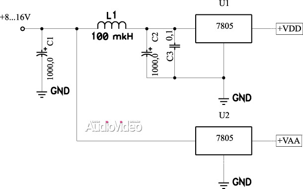
The advantages of this scheme are its simplicity and clarity. With a common rectifier, different stabilizers are used for the digital and analog parts of the circuit - this is mandatory. They are isolated from each other at the input by a filter consisting of C1, L1, C2, C3. Instead of five-volt 7805 stabilizers, it is better to install adjustable LM317s with corresponding resistive dividers in the control output circuit. Calculation of resistance values can be found in any reference book on linear microcircuits. LM317 compared to 7805 have a wider frequency range (do not forget that not only D.C., but also a wideband digital signal), less internal noise and a quieter response to impulse loads. The fact is that when a pulsed noise appears (and their power supply is visible and invisible!), the stabilization circuit, covered by deep negative feedback (it is necessary to obtain a high stabilization coefficient and low output resistance), tries to compensate for it. As expected for circuits with OOS, a damped oscillatory process occurs, on which newly arrived interference is superimposed, and as a result, the output voltage constantly jumps up and down. It follows that to power digital circuits it is advisable to use stabilizers based on discrete elements that do not contain OS. Of course, in this case, the output impedance of the source will be much higher, so all responsibility for combating impulse noise is shifted to shunt capacitors, which cope well with this task, and this has a beneficial effect on the sound. In addition, it is clearly necessary to use a separate stabilizer for each power pin of digital microcircuits along with power decoupling elements (similar to L1, C2, C3 in Fig. 2).
This is done in Markan DACs, and the filter with additional digital noise suppression and the rectifier operate from a separate winding of the network transformer, and for additional decoupling of the digital and analog parts of the circuit, different transformers are even used. The same is done to further improve our DAC, although for starters you can use the circuit in Fig. 2, it will provide an initial level of sound quality. It is better to use fast Schottky diodes in the rectifier.
Multibit version of the circuit
Typically, multibit DACs require several voltage sources of different polarities and a considerable number of additional discrete elements for their operation. Among the wide variety of microcircuits, we will choose the Philips TDA1543. This DAC is a “budget” version of the excellent TDA 1541 chip, it costs a penny and is available for retail sale in our country.
The TDA 1541 chip was used in the Arcam Alpha 5 CD player, which at one time won many prizes, although it was also much criticized - an antediluvian DAC, strong interference, but what a sound! This chip is also still used in Naim turntables. The TDA1543 is perfect for our purposes because... it requires only one +5V power supply and does not require additional parts. We unsolder the CS4390 from the digital receiver and connect the TDA 1543 in its place in accordance with the diagram in Fig. 3.
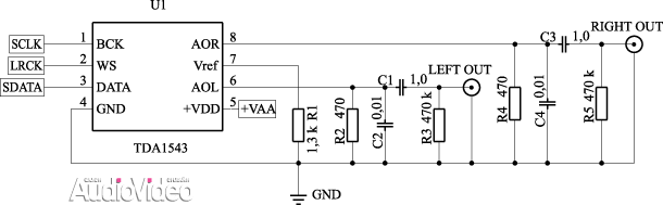
A few additional clarifications are necessary here. All multibit DACs have a current output, and several circuit solutions exist to convert the signal to voltage. The most common is an operational amplifier connected with an inverting input to the output of the DAC. The current-voltage conversion is carried out by the OS covering it. In theory, it works great, and this approach is considered classic - it can be found in the recommended options for turning on any multi-bit DAC. But if we talk about sound, then everything is not so simple. To implement this method in practice, you need very high-quality op-amps with good speed characteristics, for example AD811 or AD817, which cost more than $5 apiece. Therefore, in budget designs they often do things differently: they simply connect a regular resistor to the DAC output, and the current passing through it will create a voltage drop, i.e. full signal. The magnitude of this voltage will be directly proportional to the size of the resistor and the current flowing through it. Despite the apparent simplicity and elegance of this method, it has not yet received widespread use among manufacturers of expensive equipment, because also has many pitfalls. The main problem is that the current output of DACs does not provide for the presence of voltage on it and is usually protected by diodes connected back-to-back and introducing significant distortion into the signal received at the resistor. Among famous manufacturers Those who have decided to use this method should highlight the company Kondo, which uses a resistor wound with silver wire in its M-100DAC. Obviously, it has very little resistance and the amplitude of the output signal is also very small. To obtain a standard amplitude, several tube amplification stages are used. Another well-known company with an unconventional approach to the issue of current-voltage conversion is Audio Note. In its DACs, it uses a transformer for these purposes, in which the current passing through the primary winding causes a magnetic flux, leading to the appearance of a signal voltage on the secondary winding. The same principle is implemented in some Markan series DACs.
But let's return to the TDA 1543. It seems that the developers of this microcircuit for some reason did not install protective diodes at the output. This opens up the prospect of using a resistor current-voltage converter. Resistances R2 and R4 in Fig. 3 is just for this. At the indicated ratings, the amplitude of the output signal is about 1 V, which is quite enough to directly connect the DAC to a power amplifier. It should be noted that the load capacity of our circuit is not very high and under unfavorable conditions (high capacitance of the interconnect cable, low input impedance of the power amplifier, etc.), the sound may be slightly compressed in dynamics and “smeared”. In this case, the output buffer will help, the circuit and design of which you can choose from many existing options. It may happen that in some manufactured versions of the TDA 1543 microcircuit, protective diodes are still installed (although there is no such information in the specifications, and we also did not come across specific examples). In this case, it will be possible to remove a signal from it with an amplitude of no more than 0.2 V, and you will have to use an output amplifier. To do this, it is necessary to reduce the value of resistors R2 and R4 by 5 times. Capacitors C2 and C4 in Fig. 3 form a first-order filter that eliminates high-frequency interference from the analog signal and forms the desired frequency response in the upper part of the range.
Many DAC designs use digital filters, which greatly simplifies the developer’s task when designing the analog part, but at the same time, the digital filter bears most of the responsibility for the final sound of the device. Recently, they have begun to be abandoned, since a competent analog filter effectively suppresses high-frequency noise and does not have such a detrimental effect on musicality. This is exactly what is done in Markan DACs, which use a conventional third-order filter with linear phase characteristic, made on LC elements. In our diagram in Fig. 3, for simplicity, a first-order analog filter is used, which in most cases is quite sufficient, especially if you use tube amplifier power, and even without feedback. If you have transistor equipment, then it is quite possible that you will have to increase the order of the filter (however, do not overdo it, a circuit that is too steep will definitely worsen the sound). You will find the corresponding diagrams and formulas for calculation in any decent amateur radio reference book.
Please note that resistors R2, R4 and capacitors C2, C4 are located exactly in the place where analog sound originates. High End starts from here and, as they say, “further everywhere.” The quality of these elements (especially resistors) will greatly depend on the sound of the entire device. Resistors must be installed in carbon BC, ULI or boron-carbon BLP (after selecting them according to the same resistance using an ohmmeter), the use of imported exotics is also welcome. Capacitors are acceptable of any type listed above. All connections must be of a minimum length. Of course, high-quality output connectors are also necessary.
What did we get?
I used to sing verses badly,
wheezed, screamed and lied...(J.C. Jerome, "Three in a Boat"
not counting the dog")
I will not be lazy to remind you that before turning on the device for the first time, you must carefully check the entire installation. In this case, the amplifier volume control should be set to the minimum position and the volume should be gradually increased if there is no interference, whistling or background noise at the output. Be careful and careful!
In general, single-bit DACs are characterized by a very soft, pleasant sound, with an abundance of subtle details. It seems that they throw all their sound potential to the aid of the soloist, pushing other participants in the musical work somewhere into the background. Large orchestras are somewhat “reduced” in the composition of musicians, and the power and scale of their sound suffers. Multibit DACs pay equal attention to all participants in the musical action, without alienating or highlighting any of them. The dynamic range is wider, the sound is smoother, but at the same time somewhat more distant.
For example, when playing the well-known song “I Put A Spell on You” performed by Creedence Clearwater Revival through a multi-bit DAC, its energy is perfectly conveyed, the powerful flow of emotions is simply mesmerizing, the intention of its creators becomes clear, we acutely feel what they wanted to tell us. Small details are somewhat blurred, but against the background of the dominant characteristics of such sound delivery described above, this does not seem to be a serious drawback. When playing the same song through a one-bit DAC, the picture is somewhat different: the sound is not so large-scale, the stage is somewhat moved back, but the details of sound production and small touches are clearly audible. The moment when the musician brings the guitar closer to the amp, achieving easy self-excitation of the amplifier, is conveyed well. But when listening to Elvis Presley, all the richness of his voice is magnificently revealed. It is clearly noticeable how it changed with age, the emotional impact on the listener is also strong, and the accompaniment, somewhat relegated to the background, fits organically into the overall picture.
So the choice of DAC type is up to you; both options have both strong and weaknesses, the truth, of course, lies somewhere in the middle. Despite their simplicity, the sound potential of the described circuits is quite high, and if the given recommendations are creatively followed, the end results should not disappoint you. We wish you success!
Questions from the circuit developer
The main thing in our business is to take the right start! I don’t have to worry about building a product line from cheap consumer goods to the very high-end. Therefore, I can afford to immediately choose the digital-to-analog converter chip I like and build a design around it. So, the “mystical DAC” was taken as the basis " as it is called on the Internet. I will not make a big secret out of a small microcircuit, but let’s still keep the intrigue for a start.
Build a good DAC I’ve been planning for my beloved since the last century, but somehow I didn’t get around to it and more priority tasks took over. And here, to my delight, a customer appeared, on the one hand, able to appreciate good sound, on the other hand, willing to put up with a certain level of “homemade” in the finished device. Naturally, I will make every effort to ensure that my clients are satisfied with their choice. What my “pre-production” products lose in comparison with serial devices of popular brands is:
- part of the editing is done with cobwebs on mole rats, and not on print, which has a positive effect on the sound quality, but, alas, will not be available in production samples;
- I don’t skimp on little things like a surge protector or shunt capacitors, which, by the way, has been caught by recognized authorities more than once;
- My “brand” is not yet very widely known in narrow circles :)
Let's start, pay attention...
Where to start? That's right, it's best to start with a ready-made device, even a simple one, but containing key components. In China for US $ 50 I purchased a generally good kit for self-assembly of a DAC. As I already said, the Chinese economic genius is not distinguished by any special technical talents, so everything in that set was at a minimum, exactly according to the datasheets. Except that the creators of the set built the food, as it seemed to them, of very high quality: they stuck " KRENOK" with garlands. But the kits came with very appropriate R-core transformers.
![]()
At this stage, the task was not to somehow specifically control the digital receiver or DAC, so the hard-wired minimalist S/PDIF->I2S->DAC chain suited me quite well.
I didn't consciously try to find a DAC with a USB input. The reason is simple: the computer generates a lot of noise and there is no desire to let all this garbage into the audio device. Of course, there are methods, but I still haven’t come across a single DAC with proper decoupling of the USB input (devices for 1K green and higher, as well as products from Russian “left-handed” audio don’t count).

I consider it necessary to note that despite all my quibbles about the circuit design, etc., the quality of the printed circuit board is simply excellent!
Taking control of the situation into our own hands
In the documentation for the DAC, in one place it is written that the analog power leg must be bypassed with an electrolyte of 10 μF and ceramics of 0.1 μF. In the diagram, leg 18 is bypassed exactly like this.
 A little further in the same document it is said that it is advisable to bypass the input on pin 17 with an electrolyte of 10 μF and ceramics of 0.1 μF. The developer acted in full compliance, a dutiful comrade, just great!
Another place in the documentation says that 17 leg Can run it straight to analog power. This is what we see in the diagram :)
What’s funny is that not only in the circuit, but also on the printed circuit board, everything is laid out like this: with two electrolytes and two 0.1 μF capacitors, with a short one right between the 17th and 18th legs of the chip (the path to the capacitors from the 17th leg goes under the chip body) :

Everything came just this dirty from the factory. How I washed it is a different story :)
For those who are especially curious: the pitch of the legs of the microcircuit body is 0.65mm.
I once came across a gorgeous picture from my friend Vadich-Borisych on VKontakte: " resistance is futile". Here, it inspired me, it is as useless here as the duplicated shunt capacitors in the diagram above, I redrawn the “circuit” especially for you:

I needed to control what was happening on the 17th leg. I had to cut him alive. It’s good that they haven’t put a jumper under the chip yet - the prospect of unsoldering one leg of the SSOP case is somehow not encouraging.

Mediocrity goes overboard
What digital-to-analog converter is complete without operational amplifiers?
That's right, only high quality DAC. So I simply did not solder the modest filter on the NE5532. Maybe it was worth it to have something to listen to for comparison and make sure how unconvincingly deep loop-backed op-amps play... But I already have a CD player from a venerable manufacturer, which very diligently plays the very mediocre sound of op-amps, although hidden behind the sonorous name HDAM and soldered into small screens. And there are plenty of other similar “samples”.

Study, study, and... think!
 Perhaps on all, without exception, DACs from manufacturers from the “heavenly Empire” I see the same locomotives from “KRENOK” (the photo on the right is not mine, caught on the Internet). By fanning out serial voltage stabilizers, the developers are obviously trying to achieve better power supply isolation and reduce the penetration of interference from the digital part to the analog part. Unfortunately, the masses lack what I call “current thinking” in circuit design. In fact, everything is simple and... a little sad.
Look at some LM317 from the output side. You will probably find a 10 µF electrolyte and a few other small containers. Now let's estimate the time constant in this circuit: just look at the datasheet and make sure that the output resistance of the "crank" is very small, which is what the developers of the integrated stabilizer sought. To be honest, I’m too lazy to count now, but interference with frequencies from, say, 100 kHz and below the roll “sees” right at its output, that is, the control electrode and, as it was designed, transmits these pulsations “upstream on command,” diligently trying to maintain the voltage on its way out.

Current fluctuations reach the output of a higher voltage stabilizer. Following the same logic, fairly high-frequency current changes still flow almost unhindered throughout the entire chain of stabilizers. And they whistle and make noise to everyone around.
I see the only rational grain in the use of two linear stabilizers in a row is that small precision stabilizers usually do not tolerate high input voltages, and kits for self-assembly of DACs often fall into the hands of soldering riggers, who often do not even bother to look into documents for the used components. And the kits should still work...
The spread of sufficiently high-frequency interference can be easily prevented by adding... ordinary resistors to the circuit. Simple RC filters by entrance linear stabilizers will provide excellent decoupling of RF ripples in both directions, sharply reducing the “distance” in the circuit where surge currents reach (including the “ground” wire!)
So the power supply has undergone major changes on the board. Alas, it was not without a couple of cut tracks and hanging installation.

Sometimes a small resistor is much more effective than a large capacitor:

We respect the heritage of our ancestors
Instead of a stupid bridge, we put super-fast diodes in the rectifier, which significantly reduces the current “shocks” when the diodes are turned off. This technique is quite popular and quite meaningful, so we will use it too:

By the way, it is precisely the lack of understanding of how to decouple linear stabilizers at HF that leads meticulous developers to start installing a separate transformer for each block of the circuit. Another very popular, but also costly solution to the problem of series stabilizers: the use of current source-parallel stabilizer combinations. In this case, everything is in order with the decoupling, but the power has to be dissipated with a considerable margin.
Let's not demand too much from the "whale"
A separate article is needed to describe a series of experiments with various stabilizers. Here I’ll just note that, to the credit of the developers from the Middle Kingdom, the LDO stabilizer they chose, lm1117, may best option from commercially produced and relatively affordable integrated stabilizers. All sorts of 78XU, LM317 and others like them simply rest due to the incongruously high output impedance (measured at 100 KHz). Alas, the precision LP2951 went into the same basket. The TL431 behaves a little better in a shunt stabilizer circuit, but it has its own story: TL431 can be very different, depending on who made them. 1117 wins by a landslide. Alas, it also turns out to be the noisiest stabilizer. It rumbles and squeaks, both with and without load.
I had to assemble the stabilizer myself, using discrete components. From just two modest transistors, following the HotFET ideology, we managed to “squeeze out” everything that in an integrated design requires dozens of transistors and still falls short. Of course, to ensure the work of the “sweet couple”, several more active components were required... but that’s again a completely different story.


An interesting result of macro photography: I didn’t notice with the naked eye that the board was not completely washed off from the flux.
Polymers rule the roost
The latest modification aimed at achieving the most accurate sound transmission was the “smoothing” of the power supply.
In critical places, the usual (albeit good ChemiCon) aluminum electrolytes from the kit were replaced with solid-state aluminum Sanyo OS-CON. Since I collected two identical sets in parallel, it was possible to arrange “A/B” testing. The difference is barely audible, but it is there! Without a signal with conventional electrolytes, at (very) high gain, there was a certain “noise space” in the headphones. Polymer electrolytes take us into the absolute.
 Sanyo OS-CON - purple barrels without a notch on the lid.
If you don't want to think with your head, work with your hands
 On almost all boards and DAC kits using the CS8416 digital receiver, the Chinese put a toggle switch so that the user can choose between an optical and copper S/PDIF input (the photo on the right is a typical example caught on the Internet). So: there is no need for a switch there, the receiver chip can easily listen to two inputs without any outside help, be it a crude toggle switch or a smart microcontroller.
I’m sharing with you a trick I spotted on a demo board from Cristal Semiconductor themselves. It is enough to connect, for example, copper S/PDIF to RXN, and the output of the optical TOSLINK receiver to RXP0.

I hope there is no need to explain how this works? 😉
Even in the reference design, the companies screwed up and forgot the shunt capacitor in the TORX power supply 🙁
Economy or illiteracy?
It can be very useful to read the documentation of manufacturers, especially those that make the very microcircuits that audiophiles then swear by. I’m revealing the most secret secret: reference design board, evaluation board and similar “probes” from manufacturers usually contain examples literate the use of those same microcircuits. Moreover, it is not at all necessary to buy all these boards, and the price tags for such “samples” can be very different: 50, 400, and can exceed a thousand greenbacks. But, my dear developers, the documentation for all these boards is publicly available! Okay, good to teach.
So, what the Chinese did not read, or what they saved on: modest shunt ceramic capacitors of 1000 pF in parallel to 10 μF and 0.1 μF. It would seem - why, because with such capacitors we bypass frequencies from tens of megahertz and higher. The audio range is considered to be up to 20 kHz, well, up to hundreds of kHz. But no one has canceled the digital part in the digital-to-analog converter. So it is precisely the interference at tens of megahertz that freely walks through inexpensive self-built DACs, causing all PLLs to tremble in fear and thereby creating ideal conditions for the occurrence of terrifying JITTER.

Another popular way to save on matches
The vast majority of manufacturers of both digital audio sources and digital-to-analog converters save 30...50 cents on each device. We, the users, pay for this. Read details.
What's high-end without lamps?
 I am amused by the hordes of tube-DAC and tube-headphone-amplifier "s in the price range from one and a half hundred to hundreds of dollars that have flooded the market recently. People seem to like how a light bulb hisses and distorts at 15...24 volts anode. However, analysis of all the problems of such DACs and pseudo-tube amplifiers for headphones is a topic for a separate article, but not just one.
(photo on the right is an example, I don’t have such a lamp-tac)
Rich topic. I just skimmed the surface here and didn’t touch on the analog part at all. And how interesting it can be to properly lay out the “ground” or organize simple and yet convenient control of the device. And what are the attenuators worth - after all, you can choose them with different resistances, build them according to different topologies, and include them in different parts tract. Coordinating sources with load is a very, very interesting question, you know!... But for today it’s time for me to wrap up.
BOM, or Bill of Materials
Of course, the matter is not limited to fifty dollars. The ceramic capacitors from the kit were replaced with film. Schottky diodes, high-quality electrolytes, and a lot more had to be added, not to mention the housing. And, of course, my HotFET amplifier: only 2 (two) amplification stages from the DAC output to the headphones or amplifier output. Neither more nor less, but in the amplifier itself I counted 32 transistors in the stereo version. Yes, all transistors are JFETs and depletion MOSFETs. No way I can’t fit into the green fifty kopecks even in terms of components 🙂 Note that this is without any audiophile esotericism. Well, yes, I also have my own opinion on this matter. After all, there are people who believe that by installing the “right” components, any circuit can be made to sound. If you, dear reader, are from their ranks, teach me, I will listen, argue, listen and tell everyone about my experiences right on this site.
So where is the promised freebie???
Friends, this article is just thoughts, notes in the margins, it was written hot on the heels of remaking a Chinese DAC. I myself would never get involved in such an adventure again: although it turned out well, it was too expensive in terms of time and effort. And I don’t recommend it to anyone. When I dealt with that set, the poison simply oozed out, which was reflected in the article :) I apologize for the slightly arrogant style of presentation, and if I did not live up to your expectations and did not offer the distribution of almost free high-end DACs to the population 😉
If you were interested, please let me know. There is still a lot of material in the bins, but the strength, motivation to publish and formalize all this comes mainly from reviews and comments from my readers.
In recent decades digital audio equipment is developing at a rapid pace. In addition to the emergence of a wide range of digital amplifiers, new digital audio formats are also emerging. On the one hand, lovers of high-quality sound are pleased with the increase in sound quality, but on the other hand, they are saddened, since due to the introduction of new formats they have to constantly update their audio system.
The situation can be saved by having a separate digital-to-analog converter(DAC). To switch to a new format, you will only have to update it, and sometimes it will be enough to update only one of its blocks, for example, the S/PDIF receiver. In addition, a stand-alone DAC has another advantage - it is a universal unit and allows you to connect various digital sources from a CD / DVD player, computer or network player to your audio system.
This article describes the circuit and design of a DAC capable of operating at sampling rates of 32-96 kHz. The author deliberately did not implement support for the 192 kHz standard, since he considers it to be less widespread. The main emphasis in this device is on uncompromising quality. The element base used is not very new, but accessible. Surely, many radio amateurs have most of the components in their bins, which will allow them to easily repeat this design or upgrade the existing DAC to a higher level.
DAC SPECIFICATIONS
Functions and capabilities:
- coaxial and optical inputs,
- works with sampling frequency 32-96 kHz,
- 2-digit sample rate indicator,
- 8x oversampling,
- 24-bit digital filter,
- 24-bit digital-to-analog converters,
- digital de-emphasis (predistortion correction),
- switchable analog filters of the third order (Bessel and Butterworth),
- separate power supply for digital and analog circuits.
Technical Parameters:
| rated output voltage | 2.1V (RMS) |
| rated input voltage coaxial input |
0.5 V (resistance 75 Ω) |
| frequency range (–3 dB) | 0–fs/2 (fs=32/44.1/48 kHz) |
| 0–42 kHz (fs=88.2/96 kHz) | |
| analog filter cutoff frequency | 26 kHz (Butterworth for frequencies fs=32/44.1/48 kHz) |
| 42 kHz (Bessel for frequencies fs=88.2/96 kHz) | |
| output impedance | 100 Ω |
| signal-to-noise ratio | ≥ 114 dBa |
| distortion+noise | 0.0016% (44.1 kHz, 16-bit) |
| 0.001% (48 kHz, 24-bit) | |
| 0.0008% (96 kHz, 24-bit, b=22 kHz) | |
| intermodulation distortion factor (60 Hz/7 kHz, 0 dB) |
0.0035% |
| channel separation (1 kHz) | >115 dB |
| dynamic range | >100 dB |
The measurements were carried out at the following switch positions (see below):
| s1 | s2 | s3 | s4 |
| -1 off | -1 on | -1 on | -1 off |
| -2 off | -2 off | -2 on | -2 off |
| -3 off | -3 off | -3 on | -3 off |
| -4 on | -4 off | -4 off | -4 on |
| -5 on | |||
| -6 off | |||
| -7 off | |||
| -8 off |
BLOCK DIAGRAM
The DAC design is made in the form of 4 blocks, each of which is assembled on a separate printed circuit board:
- power supply ± 12 V and +5 V,
- digital receiver and display driver,
- 2-digit display,
- digital filter, direct digital-to-analog converter and output analog filters.
The block diagram is shown in the figure:

click to zoom
The power supply consists of a +5 V voltage regulator for the digital circuits (receiver and digital filter) and a ±12 V voltage regulator for powering the analog circuits and relays. In addition, from these voltages, with the help of additional stabilizers, voltages of ±5 V are obtained to power the DAC chip.
The digital audio receiver board also contains a display driver that allows you to control the frequency of the clock signal. The display itself consists of two 7-segment LED modules to indicate the sampling rate: 32 kHz, 44 kHz (44.1 kHz in reality), 48 kHz, 88 kHz (88.2 kHz in reality), or 96 kHz.
For the hardware configuration of the receiver, a 4-pin DIP switch is used. The reference clock signal is generated by a high-precision 6.144 MHz crystal oscillator to determine the frequency of the input signal and the phase-locked loop (PLL).
At the receiver output, data on the sampling rate and status bits are present in a mixed form. To separate them, IC5 is used. The output data is written to the registers of the microcircuit and in normal mode the output signals are static. Such indication (versus dynamic) requires much less current and, as a result, creates less interference.
A 10-core flat cable is used to connect the digital receiver board to the display board. The receiver board is connected to the DAC board and output filters using a 16-core flat cable. The same cable transmits +5V voltage from the receiver board to power the digital filter, as well as a switching signal to the output filter with double the medium frequency if a signal with frequencies of 88.2 kHz or 96 kHz is detected at the input.
The “MUTE” signal is generated when there is no signal at the receiver input or when the PLL system cannot lock the frequency. It is removed from pin 5 (ERF) of IC1 and is used to control the output relay (turns off the DAC output).
The receiver and digital filter reset signal forms R6-C13 and is inverted by IC5. The signal of the presence of dampening from the digital receiver is transmitted to a digital filter, which provides distortion correction. Twelve DIP switches allow you to set various filter parameters: input and output data formats, number of bits, filter characteristic, and others.
The digital filter controls two DAC chips: one for the left and one for the right channels. The output signal of each DAC is current. This choice was not made by chance. The current output provides good linearity, low noise, low offset voltage and high slew rate. Yes, usually DACs with current output are more expensive, but the sound quality (as a rule) is provided at a higher level.
An analog output filter is required to remove residual oversampling products and high-frequency noise from the output signal. To expand the range of sampling frequencies, the circuit uses two output filters with different cutoff frequencies. Filter switching is carried out using two relays. Since the filter resistance is high enough, it was necessary to use a separate relay for each channel so as not to worsen the channel separation.
The output impedance of the filter is only 100 Ohms, so to implement the “MUTE” function, you can use one relay without degrading the device’s performance. This function allows you to get rid of clicks and noise at the device output during transient processes when turned on or errors in reading input data.
CIRCUIT DIAGRAM (DIGITAL RECEIVER)
Schematic diagram The digital receiver and display driver block is shown in the figure:

click to zoom
The main task of the digital receiver IC1 is to decode the S/PDIF data stream into a serial data format that can be transferred to the DAC chips. The receiver chip is located on a separate printed circuit board so that the coaxial and optical input connectors can be placed in the most convenient location on the device body.
The input impedance, which has a traditional value of 75 Ohms for a coaxial input, is determined by the value of resistor R1. The optical input is implemented on the widely used IC2 chip. The signal from its output is fed to the input of IC1 through a divider R1-R2, the resistor values of which are selected in such a way that the signal at R1 is slightly larger (0.6 V) than the standard value for the coaxial input (0.5 V).
When using an optical input, jumper JP1 must be installed. The coaxial input cannot be used in this case!
Resistors R7-R10 are necessary to eliminate high-frequency “ringing” caused by the capacitive load formed by the connecting cable and the input capacitance of the digital filter.
The operating mode of the digital receiver is set by the levels at the inputs M0-M3. More details about operating modes can be found in the reference manual for the CS8414 chip. The recommended mode is I2S, since in this mode the number of bits is not fixed in principle: it can be 16-bit data or 24-bit. Therefore, it is necessary to set the DIP switches S1 to S1-4 ON (M1 = 1) and the others OFF (M0 = M2 = M3 = 0).
The ability to select different operating modes of the digital receiver was designed taking into account possible future expansion of functionality or design updates. This also allows you to use the receiver board to work together with other types of DACs.
To reduce noise and interference, the quartz oscillator chip IC3 is located as close as possible to the corresponding input (FCK) of the IC1 chip, and the power bus is equipped with a filter on elements L3, C10, C11. Separate filters are also installed in the power buses of other microcircuits.
From the outputs of the demultiplexer IC5 through connector K2, the signals (as well as the +5V supply voltage and the common wire) are sent to the display unit, which is connected to the receiver board with a 10-core cable. To simplify the circuit and reduce switching circuits, a two-digit seven-segment indicator is used, so the decimal point and fractional parts for some input signal sampling rates are omitted. If an error occurs in reading the input data (ERF signal is active), two dashes will appear on the display. Due to the placement of the display unit on a separate printed circuit board, it is convenient to mount it in any suitable location behind the front panel of the device.
Information about clock frequency The input signal is used not only for indication, but also to control the cutoff frequency of the DAC output analog filters.
The signal about the presence of predistortions in the recording from the receiver output is fed to a digital filter. There is no indication of this mode, since CDs with such recordings are quite rare. But since they exist, this DAC has the ability to process any predistortions, and processing them in a digital filter allows you to get rid of the need to switch additional RC circuits in the analog filter.
To be continued...
The article was prepared based on materials from the magazine “Elector”,
free translation by the Editor-in-Chief "Radio Newspapers".
The simplest digital-to-analog converter (DAC) is a single-bit converter. A simple amplifier-limiter can serve as such a DAC, which can be used. One made using CMOS technology is especially suitable, since in this technology the output currents of one and zero are equal. Such a digital-to-analog converter is shown in Figure 1.
Figure 1. Schematic diagram of a single-bit digital-to-analog converter (DAC)
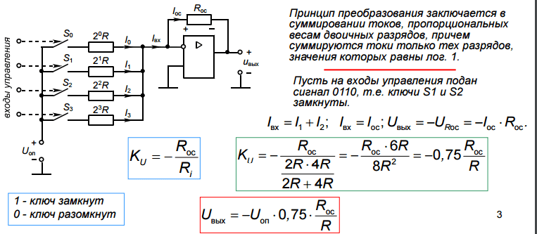
A single-digit DAC converts the sign of a number into analog form. For digital-to-analog conversion at a very high sampling frequency, many times higher than the Kotelnikov frequency, such a converter is quite sufficient, however, in most cases, for high-quality digital-to-analog conversion, a larger number of bits is required. It is known that a binary number is described by the following formula:
(1)To convert digital binary code into voltage, you can use this formula directly, that is, use an analog adder. We will set the currents using resistors. If the resistors differ from each other by a factor of two, then the currents will also obey the binary law, as shown in formula (1). If a logical one is present at the output of the register, it will be converted into a current corresponding to a binary bit using a resistor. In this case, the voltage will work as a digital-to-analog converter. The circuit of a DAC operating according to the described principle is shown in Figure 2.
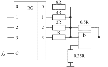
Figure 2. Schematic diagram of a four-bit digital-to-analog converter with summation of weight currents
In the diagram shown in Figure 2, the potential of the second terminal is zero. This is achieved by parallel negative feedback, which reduces the input impedance of the op-amp. The transfer coefficient is selected using a resistor connected from the output to the input of the operational amplifier. If a unity transfer coefficient is required, then this resistance should be equal to parallel resistance all resistors connected to the outputs of the parallel register. In the described device, the low-order current will be eight times less than the high-order current. To reduce the influence of input currents of a real operational amplifier, a resistor with a resistance equal to the parallel connection of all other resistors is connected between its non-inverting input and the common wire.
Considering that at the output of all register bits there is either a zero voltage or equal to the supply voltage, at the output of the operational amplifier the voltage will operate in the range from zero to minus the supply voltage. This is not always convenient. If you need the device to operate from a single power source, then it needs to be changed a little. To do this, apply a voltage equal to half the supply to the non-inverting input of the operational amplifier. It can be obtained from a resistive voltage divider. Zero current and one current of the register output stage in new scheme must match. Then the voltage at the output of the operational amplifier will vary in the range from zero to the supply voltage. The circuit of a digital-to-analog converter with unipolar power supply is shown in Figure 3.
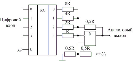
Figure 3. Single-supply D/A converter
In the circuit shown in Figure 3, the stability of the output current and voltage is ensured by the stability of the parallel register supply voltage. However, the supply voltage of digital chips is usually very noisy. This noise will also be present in the output signal. In a multi-bit digital-to-analog converter, this is undesirable, so its output switches are powered from a highly stable, low-noise converter. Currently, such microcircuits are produced by a number of companies. Examples include the ADR4520 from Analog Devices or the MAX6220_25 from Maxim Integrated.
When manufacturing multi-bit digital-to-analog converters, it is necessary to manufacture resistors with high precision. Previously, this was achieved by laser trimming of resistors. Currently, not resistors, but current generators on field-effect transistors are usually used as current sources. The use of field-effect transistors can significantly reduce the size of the DAC chip. In this case, to increase the current, the transistors are connected in parallel. This makes it possible to achieve high accuracy of current compliance with the binary law ( i 0 , 2i 0 , 4i 0 , 8i 0, etc.). High conversion speed is achieved with low load resistance. The circuit of a digital code converter into output current operating according to the described principle is shown in Figure 4.

Figure 4. Internal DAC circuit with current summation
Naturally, the electronic switches shown in Figure 4 are also field-effect transistors. However, if you show them in a diagram, you can get confused about where the key is and where the current generator is. Since a field-effect transistor can simultaneously operate as a current generator and an electronic switch, they are often combined, and the binary law is formed using, as shown in Figure 5.

Figure 5. Internal DAC circuit with summation of equal currents
An example of a chip that uses a current summation solution is the AD7945 DAC. In it, the summation of currents is used to form the most significant bits. To work with low-order digits, . An operational amplifier is usually used to convert the output current into voltage, but its slew rate has a significant impact on the performance of the digital-to-analog converter as a whole. Therefore, the DAC circuit with an operational amplifier is used only in wideband circuits such as audio or television signal conversion.
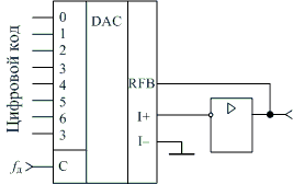
Figure 6. Digital-to-analog converter binary code-voltage
Literature:
Together with the article “Digital-to-analog converters (DACs) with current summation” read:
http://site/digital/R2R/
http://site/digital/sigmaadc.php
DAC– digital-to-analog converters – devices designed to convert a discrete (digital) signal into a continuous (analog) signal. The conversion is carried out in proportion to the binary code of the signal.
DAC classification
By type of output signal: with current output and voltage output;
By type of digital interface: with serial input and with parallel input of input code;
By the number of DACs on the chip: single-channel and multi-channel;
By speed: moderate speed and high speed.
Basic DAC parameters:
1. N – bit depth.
2. Maximum output current.
4. The magnitude of the reference voltage.
5. Resolution.
6. Control voltage levels (TTL or CMOS).
7. Conversion errors (output zero offset error, absolute conversion error, conversion nonlinearity, differential nonlinearity). 8. Conversion time – the time interval from the moment the code is presented (submitted) to the moment the output signal appears.
9. Analog signal settling time
The main elements of the DAC are:
Resistive matrices (a set of dividers with a certain TCR, with a certain deviation of 2%, 5% or less) can be built into the IC;
Switches (on bipolar or MOS transistors);
Reference voltage source.
Basic circuits for constructing a DAC.

21. ADC. General provisions. Sampling frequency. ADC classification. Operating principle of parallel ADC.
According to the speed of operation, ADCs are divided into:
1. Parallel conversion ADCs (parallel ADCs) - high-speed ADCs, have complex hardware use of the GHz unit.resolution N = 8-12 bits, Fg = tens of MHz
2. ADC of successive approximation (successive counting) up to 10 MHz. resolution N = 10-16 bits, Fg = tens of kHz
3. Integrating ADCs of hundreds of Hz.resolution N = 16-24 bits, Fg = tens
4. Sigma-delta ADC units MHz.resolution N = 16-24 bits, Fg = hundreds of Hz

22. Serial counting ADC. Operating principle.
23. ADC of successive approximations. Operating principle.

 This code from the output of the RPP is fed to the DAC, which produces the corresponding voltage 3/4Uinmax, which is compared with Uin (on the CC) and the result is written to the same bit with the fourth clock pulse. The process then continues until all digits have been analyzed.
SAR ADC conversion time:
tpr = 2nTG, where TG is the pulse repetition period of the generator; n – ADC bit capacity.
Such ADCs are inferior in speed to parallel-type ADCs, but they are cheaper and consume less power. Example: 1113PV1.
24. Operating principle of an integrating type ADC.
The operating principle of an integrating ADC is based on two basic principles:
1. Converting input voltage into frequency or pulse duration (time)
Uin → f (VLF – voltage-frequency converter)
2. Convert frequency or duration (time) to digital code
f → N; T→N.
The main error is caused by VLF.
This type of ADC performs conversion in two stages.
In the first stage, the input analog signal is integrated and this integrated value is converted into a pulse sequence. The repetition rate of pulses in this sequence or their duration is modulated by the integrated value of the input signal.
At the second stage, this sequence of pulses is converted into a digital code - its frequency or pulse duration is measured.


 Leo born in the year of the Rabbit")


 Leo born in the year of the Rabbit")
